


A well-known fact is that typical thick film hybrids are still limited by 100um line / gap design rules. An effort to achieve lower values normally requires huge investment in a precision kit of new machinery and a higher cost of exotic pastes and mesh screens. Still, the yield will be an issue.
In addition to it, multilayers with higher definition have even less chance due to the nature of the screen printed layer surface. Dried conductor has concave cross section profile with inward-looking sides. Printed lines are not straight, but have a saw-tooth effect following mesh openings in the screen. As lines go down in size this effect may completely tear them open.
Finally, achieving a higher definition in LTCC layers proves even harder.

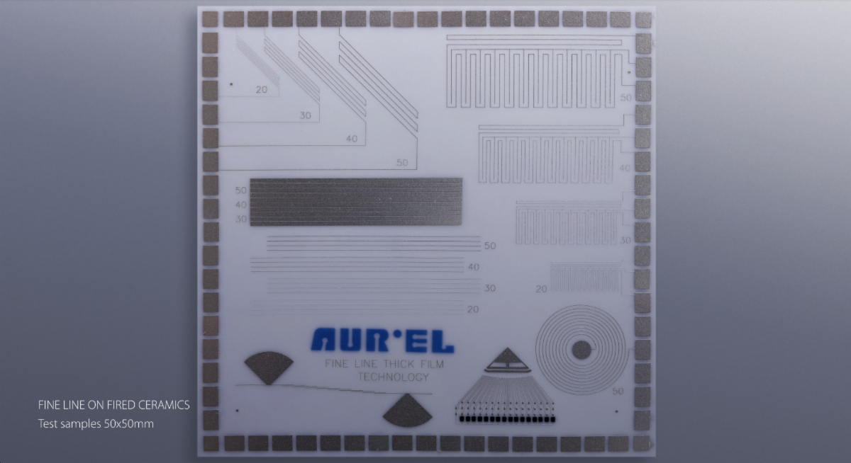
We offer our customers a cheap and reliable solution to achieve a way better resolution (typically 20um lines with 30um gaps) with the use of a standard thick film process (print-dry-fire). Our Fine Line Photoimageable Technology gives a number of exciting unmatched advantages.
It is a high yield process that can be reproduced in a volume production. Besides the fact that density of your layout can go to a completely new level with 20 um lines instead of 100 um, the lines and gaps achieved with our fine line process have strictly vertical walls and no saw-tooth effect.
Hence, RF properties of layouts are much better than of the traditional thick film. Customers get much better RF performance even staying with their approved designs (100um lines/gaps) just because of a better line geometry. Or, one can choose to redesign their products and go down to 20um lines / 30 um spaces to replace the expensive and bulky thin film elements from product design. Polished and lapped alumina substrates can give even better resolution (lines down to 10um reported at lab-scale production).
Cross section profile of fine line pastes after drying and firing is much better, without typical "valley" in the center due to photo processing. This, combined with a low viscosity of photoimageable dielectric as part of the system, allows for a high density multilayer hybrid layout with a perfectly flat top layer. It improves the yield of wire bonding and other assembly steps significantly.
Fine Line photoimageable process can be used for both fired ceramics and LTCC, thus making our customers' design rules broader. Pastes' chemistry allows for virtually any type of metal to form a fine line conductor (main compositions are silvers, silver-palladium, gold and platinum). A fine line dielectric paste completes the range, allowing for miniature vias and gaps features. Combinations of different fine line pastes (e.g., silver-palladium main tracks with gold end pads for wire bonding) were reported as successful.


More good news is that one only needs special fine line photoimageable pastes in selected high density areas - not on the entire substrate. Fine Line pastes are completely compatible with standard thick film pastes, can be fired with the same profile and furnace. This makes the technology very attractive for sensors, fan-outs and smaller elements of layout with minimal extra cost in production.


Turn Key solution will imply a kit of just two units (exposure and developer) that come as either lab-scale models, or a fully automatic systems. We take care of tooling and integration of fine line capability into the existing thick film process line.
If you are interested in our services such as Fine Line Thick Film Hybrids, Chip Resistors, Power IGBT Modules, Advanced Wire Bonding Applications, LED modules, Versatile Hermetic Packages Sealing, Automation, etc, please click here.

